Multiple choice Questions Digital Logic Design
1. How many bits must each word have in one-to-four line de-multiplexer to be implemented using a memory?
A. 8 bit
B. 4 bits
C. 2 bits
D. 1 bits
2. The total amount of memory is depends upon _________
A. The organization of memory
B. The size of the address bus of the microprocessor
C. The size of the decoding unit
D. The structure of memory
3. _____________ can be determined the Instability condition.
A. table
B. logic diagram
C. map
D. graph
4. If we add an inverter at the output of AND gate, what function is produced?
A. NAND
B. XOR
C. OR
D. NOR
5. Which is also known as coincidence detector?
A. OR gate
B. NOT gate
C. AND gate
D. NAND gate
6. Transition table include ________________
A. squares
B. oval
C. rectangles
D. circles
7. For every possible combination of logical states in the inputs, which table shows the logical state of a digital circuit output?
A. Function table
B. ASCII table
C. Truth table
D. Routing table
8. Stack is an acronym for _______________
A. Flash Memory
B. LIFO memory
C. FIFO memory
D. Bust Flash Memory
9. When an Asynchronous sequential circuit changes two or more binary states variables a Condition occurs called ____________
A. Race condition
B. deadlock condition
C. Running condition
D. None of these
10. A positive OR gate is also a negative
A. NAND gate
B. OR gate
C. NOR gate
D. AND gate
11. Sum of two octal numbers “71” and “36” = __________________
A. 123
B. 127
C. 213
D. 345
12. Time delay device is memory element of______________
A. asynchronous circuits
B. synchronous circuits
C. clocked flip-flops
D. Unlocked flip-flops
SET 2: DLD MCQs
1. Boolean algebra is also called
A. arithmetic algebra
B. switching algebra
C. Both A & B
D. linear algebra
E. algebra
F. None of there
2. Boolean function must be brought into________ To perform product of max terms
A. OR terms
B. AND terms
C. Both A & B
D. NOT terms
E. NAND terms
F. None of these
3. The binary number 10101 is equivalent to the decimal number …………..
A. 12
B. 19
C. Both A & B
D. 27
E. 21
F. None of these
4. The universal gate is ………………
A. OR gate
B. NAND gate
C. Both A & B
D. AND gate
E. None of the above
F. None of these
5. According to boolean algebra absorption law, which of the following is correct?
A. (x+y)=xy
B. x+xy=x
C. Both A & B
D. xy+y=x
E. x+y=y
F. None of these
6. A Boolean function may be transformed into
A. logical graph
B. logical diagram
C. Both A & B
D. map
E. matrix
F. None of these
7. The inverter is ……………
A. OR gate
B. NOT gate
C. Both A & B
D. AND gate
E. None of the above
8. The resulting circuit of a NAND gate are connected together is_______
A. AND gate
B. OR gate
C. Both A & B
D. NOT gate
E. None of the above
9. x*y = y*x is the
A. inverse property
B. commutative law
C. Both A & B
D. associative law
E. identity element
F. None of these
10. Minterms are also called
A. standard product
B. standard sum
C. Both A & B
D. standard division
E. standard subtraction
F. None of these
11. OR gate and __________ will form The NOR gate?
A. NAND gate
B. AND gate
C. Both A & B
D. NOT gate
E. None of the above
12. The NAND gate is AND gate followed by …………………
A. OR gate
B. NOT gate
C. Both A & B
D. AND gate
E. None of the above
13. Max terms are also called
A. standard product
B. standard sum
C. Both A & B
D. standard division
E. standard subtraction
F. None of these
14. In Boolean algebra Multiplicative inverse is
A. 1
B. 0
C. Both A & B
D. 1/a
E. a
F. None of these
15.By the repeated use of ……………… Digital circuit can be made
A. NOT gates
B. OR gates
C. Both A & B
D. NAND gates
E. None of the above
16. The only function of NOT gate is …………….. of the following
A. Invert input signal
B . Stop signal
C. both A & B
D. Act as a universal gate
E. None of the above
17. Boolean algebra is defined as a set of
A. two values
B. three values
C. Both A & B
D. four values
E. five values
F. None of these
18. First operator precedence for evaluating Boolean expressions is
A. AND
B. parenthesis
C. Both A & B
D. OR
E. NOT
F. None of these
19. The output is……………… When an input signal 1 is applied to a NOT gate
A. 1
B. 0
C. Both A & B
D. Either 0 & 1
E. None of the above
20. The bar sign (-) indicates ……………….., In Boolean algebra?
A. AND operation
B. OR operation
C. Both A & B
D. NOT operation
E. None of the above
21. The value of n is ……. when the resolution of an n bit DAC with a maximum input of 5 V is 5 mV.
A. 9
B. 8
C. Both A & B
D. 10
E. 11
F. None of these
22. 2’s complement of binary number 0101 is ………..
A. 1111
B. 1011
C. Both A & B
D. 1101
E. 1110
F. None of these
23. An OR gate has 4 inputs. The output is ……. When One input is high and the other three are low.
A. High
B. Low
C. Both A & B
D. alternately high and low
E. may be high or low depending on the relative magnitude of inputs
F. None of these
24. To convert BCD to seven segments ……………… device is used.
A. Decoder
B. Encoder
C. Both A & B
D. Multiplexer
E. None of these
25. Decimal number 10 is equal to binary number ……………
A. 1010
B. 1110
C. Both A & B
D. 1001
E. 1000
F. None of these
26. In 2’s complement representation the number 11100101 represents the decimal number ……………
A. -31
B. +37
C. Both A & B
D. +27
E. -27
F. None of these
27. BCD input 1000 is fed to a 7 segment display through a BCD to 7 segment decoder/driver. The segments which will lit up are ………….
A. a, b, c
B. a, b, d
C. Both A & B
D. all
E. a, b, g, c, d
F. None of these
28. A decade counter skips ………..
A. binary states 0000 to 0011
B. binary states 1000 to 1111
C. Both A & B
D. binary states 1010 to 1111
E. binary states 1111 to higher
F. None of these
29. ……………. Number of States A ring counter with 5 flip flops will have?
A. 10
B. 5
C. Both A & B
D. 32
E. Infinite
F. None of these
MCQs of Digital Logic Design (DLD)
Introduction to Digital Systems
- Analog vs. Digital signals MCQs
- Binary numbers and arithmetic MCQs
- Logic levels and noise margins MCQs
Boolean Algebra
- Basic logic operations (AND, OR, NOT) MCQ
- Laws and theorems of Boolean algebra MCQ
- De Morgan’s Theorems MCQ
- Canonical forms (Sum of Products, Product of Sums) MCQ
- Simplification techniques (Karnaugh Maps, Quine-McCluskey method) MCQ
Combinational Logic
Logic Gates
Combinational Circuits
- Design and analysis of combinational circuits MCQ
- Multiplexers and Demultiplexers MCQ
- Encoders and Decoders MCQ
- Binary Adders (Half adder, Full adder) MCQ
- Subtractors and Arithmetic Logic Units (ALU) MCQ
- Comparators MCQ in DLD
Sequential Logic
Flip-Flops and Latches
- SR Latch, D Latch MCQ
- Flip-Flops (SR, D, JK, T) MCQ
- Characteristic equations and excitation tables MCQ
- Edge-triggered vs. level-triggered devices MCQ
Counters and Registers
- Synchronous, Asynchronous (ripple), Up/Down counters MCQs
- Shift registers (SIPO, PISO, SISO, PIPO) MCQs
State Machines
Finite State Machines (FSMs)
Memory and Programmable Logic MCQs
Memory Devices
- Read-Only Memory (ROM)
- Random Access Memory (RAM)
- Programmable Logic Devices (PLDs) MCQs
- Field Programmable Gate Arrays (FPGAs) MCQs
More MCQs of Digital Logic Design (DLD)
- SET 1: DLD MCQs with answers (dld mcqs with answers)
- SET 2: DLD MCQs (dld basic mcqs)
- SET 3: DLD MCQs (solved mcqs of dld)
- SET 4: DLD MCQs (dld repeated mcqs)
- SET 5: DLD MCQs (dld important mcqs)
- SET 6:DLD MCQs DLD Solved MCQs Answers PDF
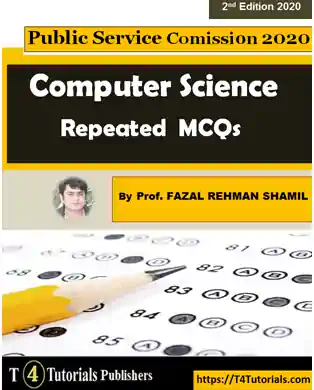
MCQs collection of solved and repeated MCQs with answers for the preparation of competitive exams, admission test and job of PPSC, FPSC, UPSC, AP, APPSC, APSC, BPSC, PSC, GOA, GPSC, HPSC, HP, JKPSC, JPSC, KPSC, KERALAPSC, MPPSC, MPSC, MPSCMANIPUR, MPSC, NPSC, OPSC, RPSC, SPSCSKM, TNPSC, TSPSC, TPSC, UPPSC, UKPSC, SPSC, KPPSC, BPSC, AJKPSC ALPSC, NPSC, LPSC, SCPSC, DPSC, DCPSC, PSC, UPSC, WVPSC, PSCW, and WPSC.