Past Guess Paper of Advanced Electronics.
Guess Paper 1 : Advanced Electronics
University Name – Confidential
NOTE: Q.1 is compulsory, attempt any four questions from the remaining. All questions carry equal marks. Phones and other Electronic Gadgets are not allowed.
Paper : Advanced Electronics
Time Allowed: 3 hours
Examination: Final, Fall – 2020
Total Marks: 70, Passing Marks (35)
Q1. (a) Explain Class A, B, & C amplifiers in detail.
(b) Explain Common-Collector amplifier.
Q2. (a) Derive a relation for total gain of 3-stage cascaded amplifier.
(b) Explain different coupling methods in amplifiers.
Q3. Explain switched capacitor DAC with the help of circuit diagram.
Q4. Briefly explain RC &LC filters with circuit diagrams used in amplifier circuits.
Q5. (a) Write a detail notes on Series and Shunt regulators.
(b) What is the difference between voltage regulators and voltage multipliers?
Q6. With the help of diagram, explain Flash A/D convertor in detail.
Q7. (a) Explain Push-Pull Amplifier in detail.
(b) Define Harmonic distortion and Feedback in amplifiers.
Q8. Write short note on any two of the following
- ADC performance and Specification.
- R-2R Ladder DAC.
- Voltage variable capacitor.
Guess Paper 2 : Advanced Electronics
University Name – Confidential
NOTE: Q.1 is compulsory, attempt any four questions from the remaining. All questions carry equal marks. Phones and other Electronic Gadgets are not allowed.
Paper : Advanced Electronics
Time Allowed: 3 hours
Examination: Final, Spring – 2020
Total Marks: 70, Passing Marks (35)
Q.1. Define the following terms properly. (14)
- Passive filters
- Uni-junction Transistor (UJT)
- Small signal and Large signal analysis (Amplifier)
- Step-up and step-down transformers
- Positive and Negative Feedbacks
- Integrated circuits (ICs)
- Cross-over distortion
Q.2. A) Define and explain switching regulators. (14)
- B) Differentiate between series and shunt regulators. Explain your answer with the help of circuits if needed.
Q.3. Convert the digital signal into analog signal using any type of combination of resistors i.e. R-2R or weighted resistor. Explain your answer with the help of equations and circuits. (14)
Q.4. Analyze the operation of RC low pass filter, and determine its critical frequency also express the voltage and power ratios of a filter in decibels. (14)
Q.5. A) Discuss the different classes of power amplifiers. (14)
- B) Class-C amplifier is the most efficient than class A, class-B or class-AB amplifiers.
- Discuss class C power dissipation
- Calculate maximum efficiency
- Calculate maximum power output
Q.6. What is Rectifier? Differentiate between half wave and Full wave rectifiers. (14)
Discuss in fully detail any two types of full wave rectifiers.
Q.7. The Light Emitting Diode (LED) is the one of the most common light sources. Explain LED for its Construction, Operation and VI-characteristics curve. (14)
Q.8. Write notes on any two of the following: (14)
- Methods of coupling
- Optoelectronic devices (Photodiode and phototransistor)
- Darlington pair
- Voltage multipliers (Doubler and Tripler)
Guess Paper 3 : Basic Electronics
University Name – Confidential
NOTE: Q.1 is compulsory, attempt any four questions from the remaining. All questions carry equal marks. Phones and other Electronic Gadgets are not allowed.
Paper : Basic Electronics
Time Allowed: 3 hours
Examination: Final, Spring – 2020
Total Marks: 70, Passing Marks (35)
Q.1 a) The series ohmmeter in given figure is made up of a 1.5V battery, a 100 microamperes meter and a resistance R1 which makes ( R1 + Rm ) = 15 kilo-ohm. Determine the instrument indication when Rx = 0
- b) Discuss the internal circuit of DC voltmeter
Q.2 a) Draw the circuit diagram of a basic two transistor flip flop. Explain the conditions that keep one transistor ON and the other one OFF.
- b) Draw the logic diagram for a general ADC.
Q.3 a) Draw the basic block diagram of a digital frequency meter, sketch the system waveforms, and carefully explain its operation.
- b) A 20V dc voltage is measured by analog and digital multi-meters. The analog instrument is on its 25 V range, and its specified accuracy is 2% the digital meter has a 3.5 digital display and an accuracy of(0.6+1). Determine the measurement accuracy in each case.
Q.4 Discuss the electronic meters for measurement of very high and very low resistances
Q.5 a) Sketch RL series and parallel equivalent circuits for an inductor.
- b) When the given circuit is in resonance. E=100 mV, R = 5 Ohms and XL= Xc= 100 Ohms. Calculate the Q factor.
Q.6 Draw the block diagram for a digital spectrum analyzer. Explain its operation.
Q.7 Explain the basic operation of a digital storage oscilloscope, and discuss the relationship between sampling rate and bandwidth.
Q.8 Write note on any TWO of the following:
- Thermocouple instruments
- Unregulated DC power supply
- Low frequency signal generator
Guess Paper 4: Digital Electronics
University Name – Confidential
NOTE: Q.1 is compulsory, attempt any four questions from the remaining. All questions carry equal marks. Phones and other Electronic Gadgets are not allowed.
Paper : Digital Electronics
Time Allowed: 3 hours
Examination: Final, Spring – 2020
Total Marks: 70, Passing Marks (35)
Q-1. Differentiate among the following terms. (14)
- Analog and Digital quantities
- OR & AND logic operations
- Multiplexer and Demultiplexer
- RAM and ROM types of memories
- Encoding and Decoding
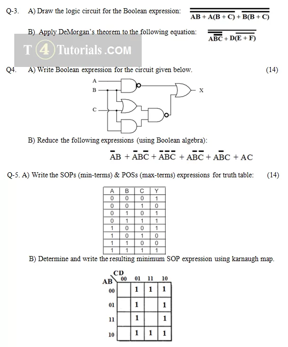
- SOP (min-terms) and POS (max-terms)
- Combinational and sequential logic
Q-2. Answer the following short questions. (14)
- (B52.F16)16 = (_________________)2
- (10010101)2 = (_________________)10
- (786.75)10 = (___________________)2
- Convert the binary number (1100011)2 to Gray Code
- 2’s complement of (100101)2?
Q-6. A) Define ADDERS. Also explain Full adder circuit using its Symbol, truth table, logic expressions and logic diagram? (14)
Q7. Define Flip-Flops, Also explain any two types of Flip-Flops? (14)
Q8. Write note on any two of the following. (14)
- Parallel Binary Adders
- Counter designing
- Programmable Logic Arrays
Guess Paper 5: Digital Electronics
University Name – Confidential
NOTE: Q.1 is compulsory, attempt any four questions from the remaining. All questions carry equal marks. Phones and other Electronic Gadgets are not allowed.
Paper : Digital Electronics
Time Allowed: 3 hours
Examination: Final, Fall – 2020
Total Marks: 70, Passing Marks (35)
Q.1. Answer the following short questions: (14)
- Differentiate between analog and digital quantities.
- Convert (5C.8)16 into binary number i.e. (——————————)
- Find the 2’s compliment of the given binary number i.e.
- The given ASCII character 00110111 is received by an odd parity system. Is it correct?
- Draw pulse/timing diagram for the number
- Add the given BCD numbers properly. 10000110+00010011.
- Draw logic diagram for the Boolean expression:
Q.2. A) Describe a Full-adder logic circuit in terms of its operation, logic diagram and logic expressions. (14)
- B) Minimize the under given SOP expression using the Karnaugh map:
Q.3. A) Differentiate between Latch and Flip Flop. (14)
- B) Describe the operation, logic diagram and truth table for JK flip-flop. Also describe that how JK flip-flop is different than SR.
Q.4. A) Design and explain the function of Decimal to BCD Encoder. (14)
- B) Convert the following Gray codes to Binary using logic gates.
- 1100011 ii. 1001101
Q.5. Differentiate between Synchronous and Asynchronous counter. Design Asynchronous counter that counts from 0 to 11 states & restart counting from 0 on its 12th state. (14)
Q.6. Explain how data bits are entered and shifted through Serial In Serial Out (SISO), and Serial In Parallel Out (SIPO) shift registers. (14)
Q.7. A) Discuss Ex-OR & Ex-NOR logic. (14)
- B) Differentiate between Multiplexer & Demultiplexer. Design 1-to-8-lines DEMUX.
Q.8. Attempt any two of the following. (14)
- What is the universal property of NAND or NOR gate? Explain.
- Describe a 3-Bit ripple/asynchronous binary counter.
- Differentiate among the TTL, ECL and CMOS integrated circuits.
- Analyze the internal logic of a magnitude comparator that has both equality and in-equality outputs.
Guess Paper 6: Basic Electronics
University Name – Confidential
NOTE: Q.1 is compulsory, attempt any four questions from the remaining. All questions carry equal marks. Phones and other Electronic Gadgets are not allowed.
Paper : Basic Electronics
Time Allowed: 3 hours
Examination: Final, Fall – 2018
Total Marks: 70, Passing Marks (35)
Q.1 Fill in the blanks [14 Marks]
- The Naturally Pure Semiconductor is called …………Semiconductor.
- The Majority carriers in N-Type semiconductor is …………………………………
- The Device/Element have the ability of rectification is known as ______________.
- The _______ is current controlled and Uni-Polar device .
- BJT stand for_______.
- IGFET stand for………
- The SCR stand for…………………………………………………
Q.2. Discuss the Depletion region of PN Junction Diode .Also draw and Explain the PN Junction Diode VI –Characteristics Curve. (14)
Q.3. With the help of circuit diagram briefly discuss the Full wave Rectifier (Center –Tapped Transformer) in Detail. (14)
Q.4. Briefly explain that how Zener Diode is used as Voltage Regulation using Mathematically Calculation. (14)
Q.5. Briefly Explain Field Effect Transistor (FET) Construction/Structures and their basic operation. (14)
Q.6 Draw the circuit diagrams and explain Common Base, Common Emitter and Common Collector
Configuration. (14)
Q.7 Briefly discuss the construction, Operation, Voltage-Current Characteristics Curve and Practical
application of Silicon Controlled Rectifier. (14)
Q.8. Write short notes on any TWO of the following.
(a) 4-Layer Device (Shockley Device) (07)
(b) MOSFET (07)
(c) Energy Band Theory of Solids (07)
Guess Paper 7: Basic Electronics
University Name – Confidential
NOTE: Q.1 is compulsory, attempt any four questions from the remaining. All questions carry equal marks. Phones and other Electronic Gadgets are not allowed.
Paper : Basic Electronics
Time Allowed: 3 hours
Examination: Final, Fall – 2017
Total Marks: 70, Passing Marks (35)
Q.1 Fill in the blanks [14 Marks]
- The Naturally Pure Semiconductor is called …………Semiconductor.
- The Majority carriers in P-Type semiconductor is …………………………………
- The Device/Element have the ability of amplification is known as ______.
- The Diode having the ability of Voltage regulation is known as _______.
- MOSFET stand for_______.
- SCR stand for………
- The Diode Limiter is also called?
Q.2. (a) Discuss Forward and Reverse Bias of PN Junction Diode.
(b) Briefly discuss the Types of Semiconductor in detail. (4+10)
Q.3. With the help of circuit diagram briefly discuss the Half wave Rectifier in Detail. (14)
Q.4. (a) Discuss the working & construction of Special purpose diode (LED).
(b)Write down the differences between Conductors and Semiconductors. (10+4)
Q.5. Briefly Explain Bipolar Junction Transistor Construction/Structures and their basic operation. (14)
Q.6 Draw the circuit diagrams and explain Common Base, Common Emitter and Common Collector
Configuration. (14)
Q.7 Briefly discuss the construction and biasing of Silicon Controlled Rectifier (14)
Q.8. Write short notes on any TWO of the following.
(a) 4-Layer Device (Shockley Device) (07)
(b) MOSFET (07)
(c)PN junction diode VI Characteristics (07)